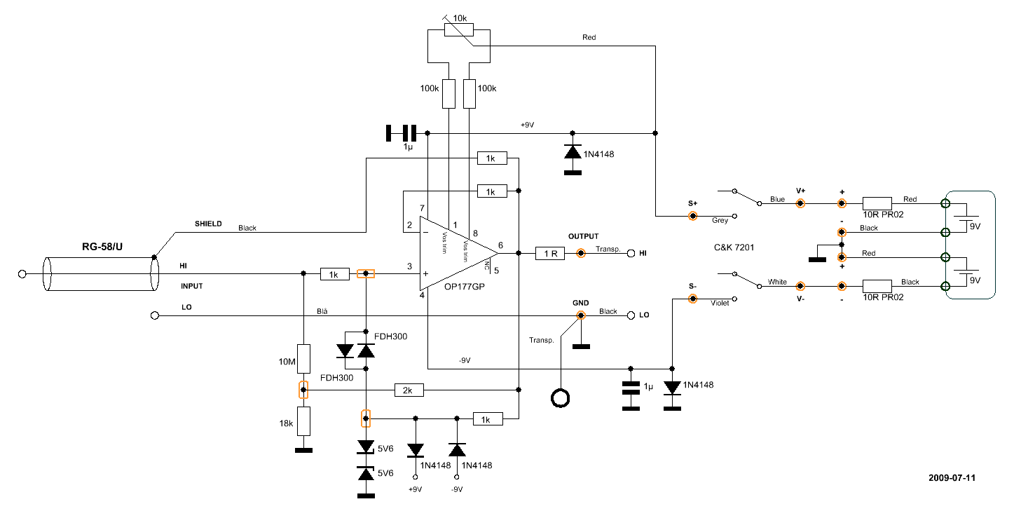
Valhalla Scientific 2009 Precision Buffer Amplifier
|
In a quest for improved precision I decided to modify my Valhalla 2009 buffer amplifier. The purpose was also to protect the amplifier against overvoltage conditions. It ended as a total new design where only the printed circuit board and the box were re-used. The new design shown on the schematic diagram here uses a bootstrapped input stage which I have used later in other designs.
The list below summarizes the changes: |
1) Amplifier upgrade from LM101AH to OP177GPZ
2) The screen for the input cable is not connected directly to the inverting input as in the original design but via a separate resistor
3) Local decoupling of supplies was added
4) A diode on both supply rails was added for a) accidental wrong polarization, and b) return route for rail current when only one battery is inserted
5) Series resistor for each supply rail added to lower the current during the switching on of the amplifier and in case of wrong polarization
6) The 1 Ohm series resistor (as indicated on the front panel) got included
7) Trimming changed to match the OP177GPZ
8) Same resistance for the inverting and non-inverting inputs of the OP177GPZ
9) Resistance added between the non-inverting input and GND to allow the flow of bias current during open input; The input impedance is determined by the bootstrap attenuation. In the above diagram the input impedance will be 100 MΩ.
10) Diode protection added to the input, with low leakage and bootstrap load reduction
Brüel & Kjær Type 2706 Power Amplifier
The Type 2706 Power Amplifier was designed to drive vibration exciters for vibration testing, and for general purpose power amplification in the audio range. The amplifier is neatly built, in the usual Brüel & Kjær manner. When putting the amplifier into use in applications for which it was not originally intended, the design has its limitations, however. For instance, the specified frequency range is 10 Hz to 20 kHz (+/- 0.5 dB), and DC-coupling may be required for preserving pulse fidelity, for driving linear actuators, etc.
I decided to give the amplifier a tech overhaul to allow operation to DC, and at the same time to squeeze out some more performance in terms of noise, distortion and bandwidth. I have not been able to retrieve a service manual for the amplifier, so the first step was to do a reverse engineering to produce some fresh schematics. Not surprisingly, the design turns out to be a rather straightforward, no-nonsense design, and quite typical for early 70's amplifiers. Features that distinguish the amplifier from common audio amplifiers of the era include the clipping detector, the switchable current limiter, and the thermal shut-down circuitry.
I started out by doing a series of measurements of the original amplifier to characterize it properly and in order to prioritize the modifications.
|
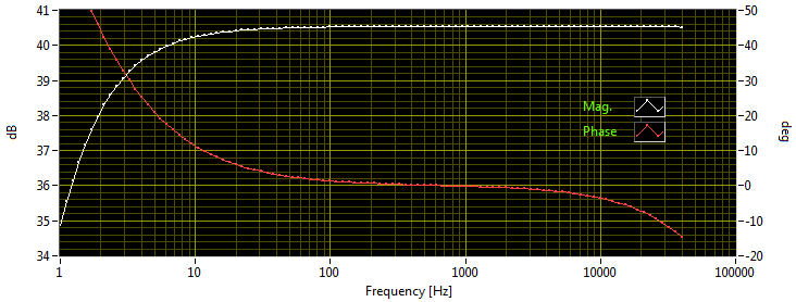
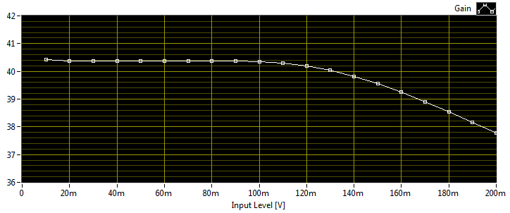
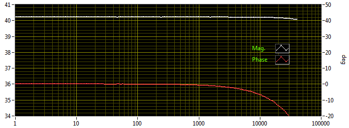
Frequency/phase response, for the original amplifier before modification, from 1 Hz to 40 kHz in 4 Ohm load, 50 mVp source amplitude. The Attenuator and the Gain Control knobs of the 2706 were set for maximum gain. The Current Limit selector was set to 5.0 A RMS. The sweep was made with the National Instruments USB-4431 DSA, using 5x attenuation between the amplifier's output and the signal analyzer's input. The gain is within the specified 40 dB +/- 1 dB @ 1 kHz.
|
|
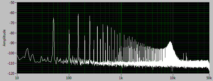
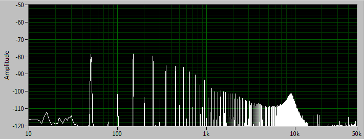
Noise spectrum, original amplifier, with shorted input. Attenuator is set to 0 dB, while the Gain Control is set to maximum. The balanced input of the USB-4431 is essential for a reliable measurement. The RMS level over a 50 kHz bandwidth is 1.53 mV, disregarding the DC-offset. The noise is dominated by mains ripple components. The 50 Hz, 100 Hz and the 150 Hz harmonic components are 0.81 mV, 0.21 mV and 1.26 mV respectively.
The RMS noise level (measured with a Fluke 8920A TRMS Voltmeter) is 2.24 mV with the Gain Control set to minimum and 2.49 mV when set to maximum. This is within the specified maximum of 4.75 mV, though no measurements conditions are stated in the "Instructions and Applications" manual. |
|
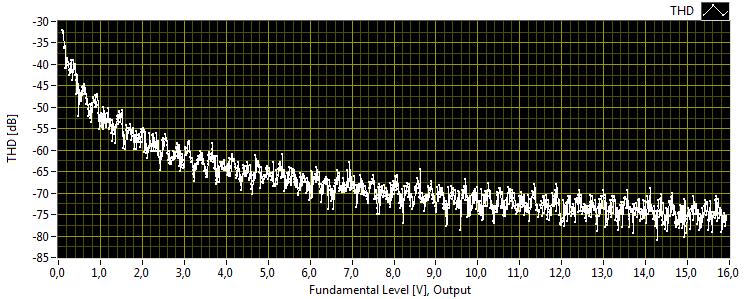
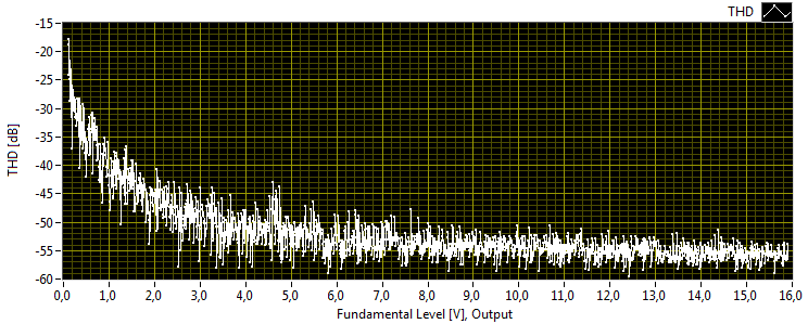
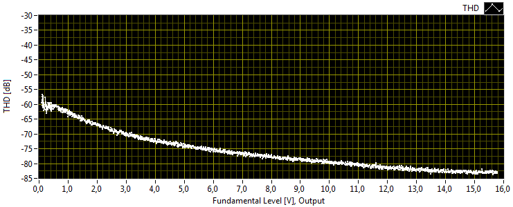
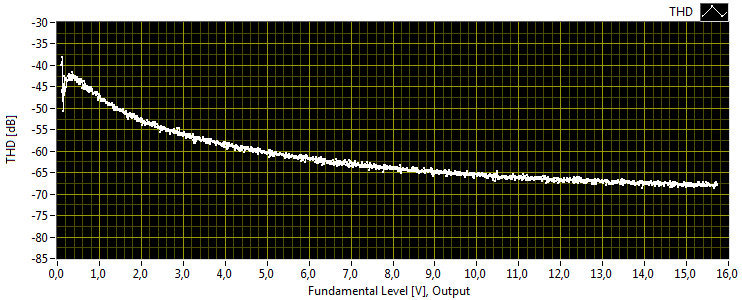
THD at 1007 Hz (measurements of THD at 1 kHz are misleading due to the high contents of mains harmonics), original amplifier, in 4 Ohms load, as a function of the output level. The 2nd to the 9th harmonic are included. The Current Limit selector was set to 5.0 A RMS. The irregular look of the curve is caused by harmonics of the mains ripple.
The measurements were done with the National Instruments USB-4431 and the LabVIEW Sound & Vibration toolkit. The signal from the output is attenuated 5 times to avoid overload of the USB-4431. |
|
THD at 10.07 kHz, original amplifier, in 4 Ohms load, as a function of the output level. The 2nd, 3rd and the 4th harmonic are included in the THD calculation. The Current Limit selector was set to 5.0 A RMS.
|
|
This graph shows the output vs. the input amplitude at 40 kHz for the original amplifier, into a 4 Ohm load. Due to slew-rate limitations the output at 40 kHz is limited to about 10 Vp.
At 10 kHz this graph is flat, corresponding to at least 20Vp capability into 4 Ohms at 10 kHz. |
|
|
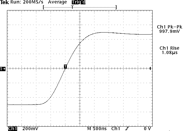
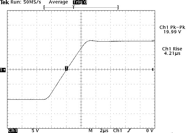
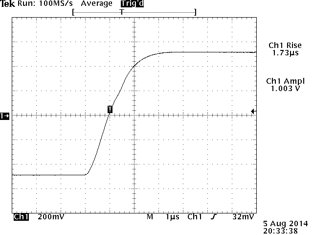
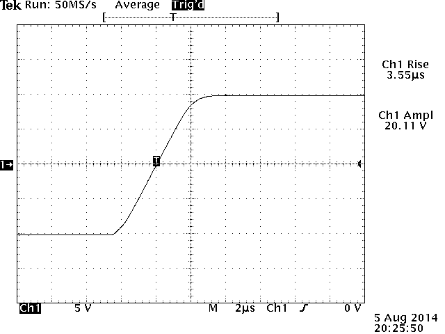
The screenshots show the rising edge at 1 Vpp and 20 Vpp output level for the original 2706 amplifier. The source is 1 kHz square wave, and the load is 4 Ohms.
The slew-rate limitation increases the rise and fall time considerably at high levels. Note the different time scale on the two screenshots. |
Summary of the observations:
- The output noise is dominated by mains ripple components, and leaves room for improvement.
- Due to the internal wiring of the 2706 the ripple currents may pollute the signal severely (about 40 to 50 mV RMS observed) if the output is connected to another instrument and a ground loop is established. The 2706 is clearly made for loads such as a exciter or a loudspeaker. A better wiring and grounding approach seems like an obvious thing to look at.
- Slew-rate limitation quickly kicks in above 20 kHz (sine wave) at the rated max. level (15 V RMS), and slows down pulse edges at large output levels.
- The pre-amplifier board with the attenuator and the level control is located close to the power transformer. The electromagnetic stray field from the transformer will inevitably generate voltages in the pre-amplifier due to the track loops. This limits how much the ripple harmonics can be reduced by re-wiring, and another pre-amplifier in combination with a shielded toroidal transformer seem to be required if lower ripple contents are called for.
The modifications include:
- Changes to the grounding wiring to have a well-defined reference point and to minimize the ripple current noise
- Added a solid ground bar for the power supply's electrolytic capacitors, with one access point for the center to reduce the ripple noise
- Decoupling of the power rails to prevent resonant rail behavior and to smoothen the open-loop response
- DC-coupling of the input and the feed-back to allow amplification to DC
- Got rid of an unwanted loop about 3 by 1½ cm made up of the lower part of the feedback network to reduce the noise pick-up
- Reduced the impedance of the input and feedback networks to reduce the effect of the bias current and to dilute the effect of any parasitic feedback capacitance
- The bootstrapped load for the voltage amplification stage was replaced with a current source to have a large open-loop gain at lower frequencies and DC, and to have a well-defined operational point
- The transistors for the long-tailed input were replaced with MAT02FH for improving the offset and drift
- Additional PNP added to input of the grounded emitter PNP voltage amplifying stage to boost the current amplification
- Bias circuitry replaced with non-switching circuitry to reduce the cross-over distortion and to stabilize the bias current and make it independent of the current limit setting
- Emitter-follower buffer inserted before the output stage to isolate the voltage amplification stage
- Compensation modified to improve the response and to widen the full-power frequency range; The open-loop response checked with a network analyzer.
- RC input filter to limit the bandwidth before the amplifier
- Relocated the AC wire for the clipping detector so it does not pass the input
- Schottky-barrier diodes added to the grounded PNP amplification stage and the current source to improve the clipping behavior
- Anti-parallel Schottky-barrier diodes added from basis to basis of the input pair to improve the overload behavior
- The input amplifier's LM301 replaced with AD711 to improve specs
- Proper grounding of the input amplifier (less pick-up of stray field form power transformer requires a new pre-amp board, though)
- Thermal shutdown circuitry on the input of the power amplifier changed to avoid DC effects
- The attenuator circuitry for the input amplifier changed to improve the accuracy of the 10 dB steps
|
This is the result of the first simple rewiring for the cold output terminal (compare with the original spectrum above).
Rather than being connected to one of the two power supply capacitors the cold terminal is now connected to the ground point on the input of the amplifier. The center of the power supply is connected to this point, too. The effect of the ripple currents is clearly reduced. The RMS level over a 50 kHz bandwidth is now 0.27 mV, a reduction of 15 dB. The 50 Hz, 100 Hz and the 150 Hz harmonic components are reduced to 0.17 mV, 12 uV and 0.18 mV. |
|
Frequency response for the modified amplifier, under same measurement conditions as above.
The response now extends to DC. There's a slightly lower roll-off frequency due to the lowpass filter inserted before the power amplifier's input. The power bandwidth, on the other hand, has been increased, as shown below. |
|
The gain compression at 40 kHz has been reduced due to the increased maximum slew-rate. The amplifier can now output about 18 Vp sine wave at 40 kHz. The different y-scale compared to the measurement of the original amplifier is caused by another setting of the attenuator.
|
|
THD at 1007 Hz for the modified amplifier, in 4 Ohms load, as a function of the output level. Though results have improved the influence of the remaining ripple still bothers this particular measurement setup.
|
|
THD at 10.07 kHz, modified amplifier, in 4 Ohms load, as a function of the output level. The 2nd, 3rd and the 4th harmonic are included in the THD calculation.
|
|
|
The screenshots show the rising edge at 1 Vpp and 20 Vpp output level for the modified 2706 amplifier. The source is 1 kHz square wave, and the load is 4 Ohms.
|
The modifications have improved the specifications, and now allow operation at DC. The ripple harmonics and the distortion have been reduced, though ripple remains an issue, apparently due to the stray field from the mains transformer. The clipping behavior is clean, and the power bandwidth extends to above 20 kHz.
It's striking that most of the improvements were possible without adding significant cost, and some were absolutely free, such as the changes to grounding and wiring. Also, all changes could in fact have been done at the time of the design in the 1970's, albeit the input op-amp and the transistor pair would have had to be different. Putting the circuit changes aside, this has first and foremost been an instructive demonstration of why you should think of wiring and grounding with diligence: Wires behave like inductive resistors, not like superconductors!
Suggestions for further improvements:
- Replace the present power transformer with a toroidal transformer in order to reduce the mains ripple harmonics.
- Add a current mirror load for the long-tailed input pair for linearity and DC stability.
