Box 73 DCF77 Frequenznormal add-ons
The frequency of the restored 10 MHz output signal from the Box 73 Frequenznormal will wobble violently if its lock speed-up circuitry gets kicked in during operation. This could happen (and does almost with certainty where I live) during periods of time where the ground wave and the sky wave interfere, typically around sunrise and sunset.
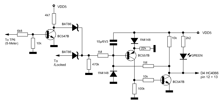
I made this circuit to prevent the PLL from going into the wide bandwidth speed-up mode once it has been in the narrow bandwidth mode. The circuit is inserted just before switch D4 so that the /Locked signal from the window detector no longer controls the switch directly. The circuit requires that both the level at TP6 and the /Locked signal are deemed OK. If so, the output control voltage for the switch D4 will go active (low) after about 4 seconds, and will then stay low. After a power cycle the control voltage will start in the inactive (high) state.
|
|
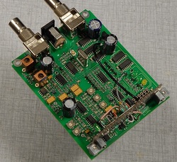
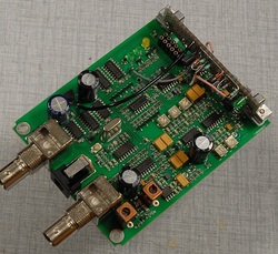
The add-on control circuit was implemented on a double-sided experimental board with ordinary leaded components, clearly more bulky than the surface mounted devices, but it served as a proof-of-concept without having to make a dedicated PCB.
The control circuit is powered from the VDD5 supply rail. You may solder a thin insulated wire to one of the vias used for the VDD5 net. I have used a via that is located close to the front edge of the receiver board (the rightmost pink wire on the left picture). |
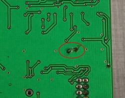
If you want to add the control circuit to your own DCF77 Frequenznormal you need to cut the track on the back of the circuit board as shown in the picture. This disconnects the switch D4 from op-amp N7 pin 7, and allows you to add a thin insulated wire from the via closest to switch D4 to the control circuit's output. The other via is then used to connect the /Locked signal to the control circuit.
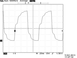
Another modification was to lower the source impedance of the 10 MHz output. In the original design, a HC04D gate drives the output through a 47 Ω series termination. However, the source impedance of the output driver for this logic family is not insignificant, and is not necessarily the same for rising and falling edges. This results in an output drive mismatch of the 10 MHz output, and you may perhaps encounter trigger uncertainties in the equipment connected to the Box 73 reference.
The picture shows the unterminated 10 MHz signal at the end of a 2 m RG-58 cable. The height of the first shoulder suggests that the total source impedance for the rising edge is close to the double of the cable's impedance. For the falling edge the total source impedance is lower.
The picture shows the unterminated 10 MHz signal at the end of a 2 m RG-58 cable. The height of the first shoulder suggests that the total source impedance for the rising edge is close to the double of the cable's impedance. For the falling edge the total source impedance is lower.
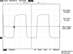
I decided to replace the 47 Ω series with an L-pad to get proper termination for both rising and falling edges, and to add protection against shorts. The L-pad consists of a 240 Ω series resistor replacing the original 47 Ω, and a parallel connection of 68 Ω and 560 Ω to ground on the output. The picture shows the unterminated 10 MHz signal with the L-pad added, using the same cable as above.
The level is reduced to about 835 mVpp, which in most cases should be of no concern. When in doubt, check if there are specific level requirements for your frequency counter, etc.
The level is reduced to about 835 mVpp, which in most cases should be of no concern. When in doubt, check if there are specific level requirements for your frequency counter, etc.
