Modifications of the Philips PM5141 LF Synthesizer
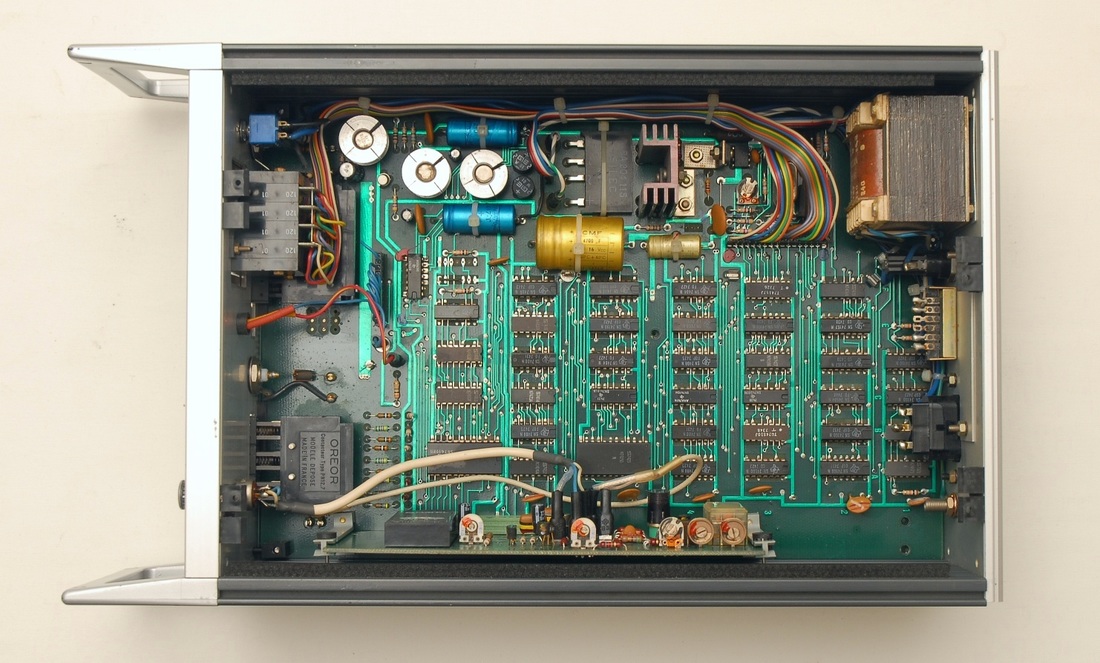
An internal view of the (unmodified) PM5141.
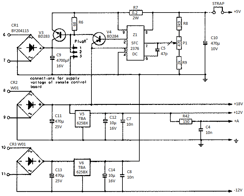
Excerpt from the schematic diagram of the PM5141. Note how excessive current from the +18V rail will pass through V4 and V3 to the +5V rail if the voltage over the storage capacitor C9 is sufficiently low.
|
The PM5141 is a synthesized LF generator with 0.01 Hz to 99.99 kHz frequency range, settable by thumbwheel switches. The PM5141 was introduced in the 1975 Philips T&M catalog. In spite of the rather outdated design with a variety of TTL-gates and a rare Datel 98BI 8-bit D/A-converter for the sine wave output, the PM5141 can still be a useful generator.
The things to look out for are: 1) Number one on the list is that the +5 V power supply is poorly designed and runs hot! The first issue is that the current for the +5 V rail will flow from the +18 V rail through driver transistor BD284 (V4) and then through the BE path of the power transistor BD283 (V3) whenever the voltage over the 4700 µF / 16 V storage capacitor (C9) is low. Take a look at the schematic diagram on the left. This not only happens when then mains voltage is low, but actually happens during parts of each ripple voltage dip over C9. Following this, the driver transistor V4 becomes unneccessarily hot. Also, it will disturb the +12 V rail, and will put additional load on the mains transformer. One remedy is to increase the value of C9 from 4700µF/16V to 10000µF/16 V so that the ripple amplitude becomes smaller, and to add a larger heatsink to the driver V4, though this does not in any way put the flawed design right. Another issue is that the heatsink for the power transistor is too small and becomes way too hot. Facing all this, I replaced all of the +5 V regulator circuitry with an integrated low-dropout regulator, the LT1084CP-5 from Linear Technology, mounted on an L-shaped aluminium profile firmly attached to the side panel. Having replaced the 4700 µF / 16 V capacitor with a new 10000 µF / 16 V, the voltage across C9 now reads 7.2 V low, 9.0 V high, at 230 VAC. At the bottom of this page you will find a picture of a modified PM5141. 2) Expect that the the thumbwheel and pushbutton switches may suffer from bad contacts. This was indeed the case with the two PM5141 units I got, but a good rinse with a contact cleaning spray did the trick. 3) There's no frequency reference input, so the frequency accuracy depends on the internal crystal oscillator. For those in need of an external reference input, take a look at the modification described below. 4) The output signal suffers from a high level of jitter, which also depends on the frequency setting. A few examples are shown below. The jitter is a result of the specific design, and there's no fix. You are encouraged to find out if this is an issue for your application! |
|
The PM5141 lacks a frequency reference input, so you're stuck with the accuracy and drift of the internal reference crystal oscillator. I had the idea that the PM5141 could serve as signal interferer for testing longwave time service receivers, and perhaps for other time/frequency related experiments. Needless to say, the ability to sync to a common reference is a must in such applications, so what to do about that?
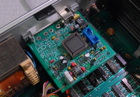
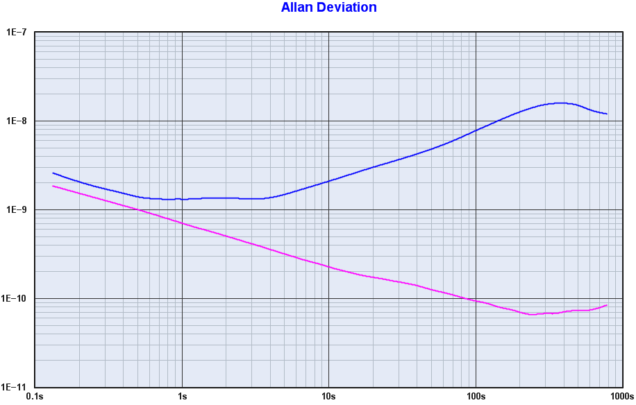
I decided to add my home-made frequency translator board to synchronize the 18 MHz reference oscillator of the PM5141 to an external 10 MHz reference. The translator board includes a complete PLL with frequency dividers and a phase-frequency detector (PFD) contained in a CPLD, and a control amplifier. The translator board also includes a VCXO, but this is not not required is this case. A capacitance diode was added to turn the reference oscillator of the PM5141 into a VCXO. With mounting brackets model 60807-181 from Schroff, the translator board fits neatly into the 70 mm spacing of the mounting holes in the back panel for the remote control option. The graph below shows the Allan Deviation for the original PM5141 with the free-running XO as reference, and for the modified PM5141 when locked to an external 10 MHz reference. In both cases the PM5141 was set to 10 kHz, and the frequency was measured for an hour with the Fluke PM6680B, the Z3805A as reference for both the Fluke PM6680A and the PM5141, and TimeLab as acquisition software. The translating PLL was designed to have 10 Hz loop bandwidth. |
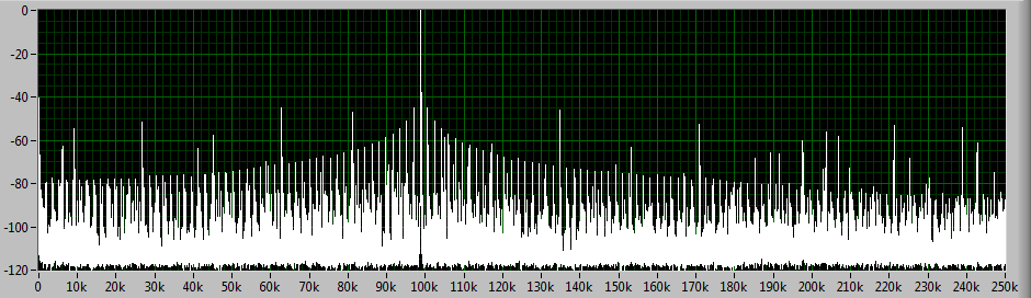
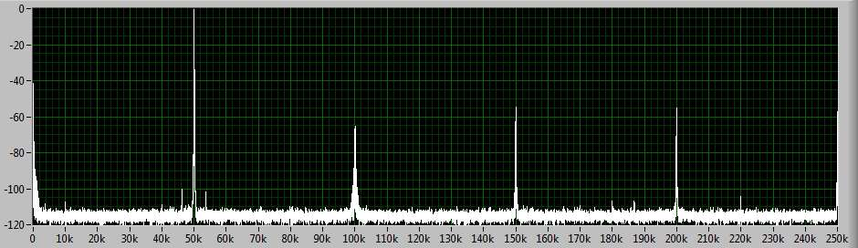
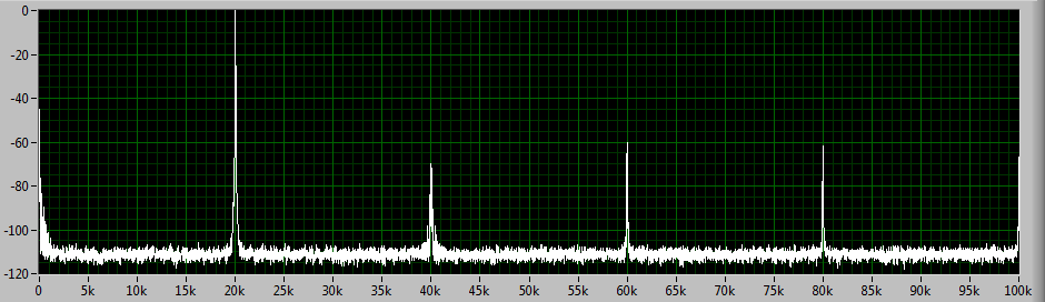
PM5141 falling edge for 98.79 kHz, and the corresponding spectrum for the sine wave output. In comparison, the spectrum for a 90 kHz setting is much cleaner due to the benign crystal clock to output integer ratio.
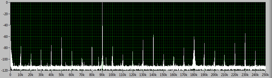
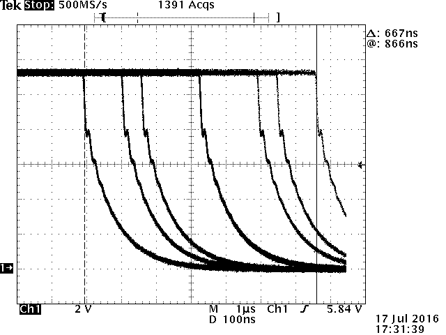
PM5141 falling edge for 45.09 kHz, and the corresponding spectrum for the sine wave output. Again, the spectrum for a 50 kHz setting is clean.
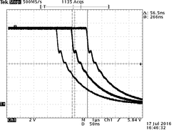
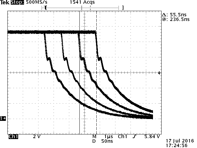
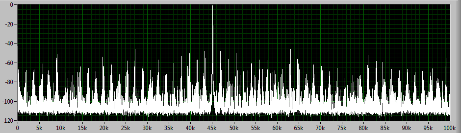
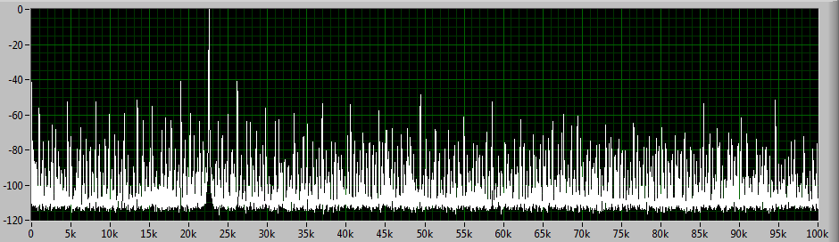
PM5141 falling edge for 22.56 kHz, and the corresponding spectrum for the sine wave output. For this frequency the jitter spans over 12 cycles of the 18 MHz clock. As expected, the spectrum is quite polluted compared to the spectrum for a 20 kHz setting.
|
Due to the design of the PM5141 there's an inherent timing jitter that equals a number of 18 MHz clock cycles. This may or may not be an issue, all depending on your requirements.
Take a look at the oscilloscope screen dumps on the left. We're looking at the falling edge following the triggering rising edge at three different frequencies for the square wave output of the PM5141. The vector accumulate display function on the Tektronix TDA340A allows us to see all locations of the falling edge. Note how the number of different locations varies. For the lower ranges the jitter remains a number of 18 MHz cycles, and will thereby become smaller in relative terms. As a result, the purity of the spectrum depends heavily on the frequency setting. The spectra for the sine wave output shown on the left, captured with an NI X-series DAQ, testify this. Only for a subset of frequency settings, with a favourable ratio between the crystal clock and the setting, you get a signal without the excessive clock period jitter, and thereby a clean spectrum. |
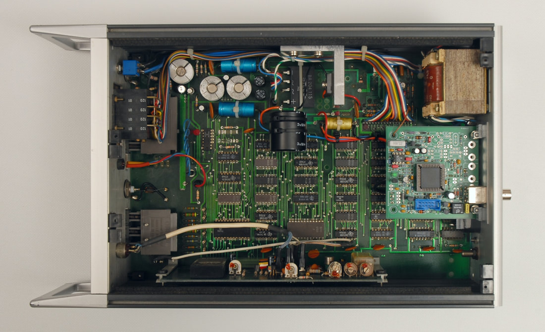
A modified PM5141, with the 10 MHz to 18 MHz PLL translator on the right, and the new +5 V power supply with the LT1084CT-5 on the L-shaped aluminium profile at the top of the picture. Two 4 mm nuts are inserted into the grooves of the side panel profiles to allow the L-shaped profile to be securely screwed into the side panel with good thermal contact. The 4700 µF / 16 V capacitor has been replaced with a 10000 µF / 16 V capacitor in order to decrease the ripple amplitude. The holes in the board under the 4700 µF / 16 V capacitor (not visible in the picture) are now used for stand-offs and cable tie anchors to keep the 10000 µF / 16 V capacitor in place.
