Repair / update: Valhalla 2701C Programmable Precision DC Voltage / Current Standard
|
(Picture to be added)
|
The 2701C is the latest edition of the 2701 references, and is still produced by Valhalla Scientific. It exploits the principle of PWM (Pulse Width Modulation) as described in the patent "Générateur étalon de tension continue ou de courant continu", by Roger Charbonnier from Adret Électronique, dated April 1st, 1966.
I found a unit offered as "Not Working, For Parts" which caught my interest. With schematics available on the Internet I did not hesitate and placed a bid, and won. The shipping and tax about doubled the price, but in all I found the cost reasonable. The 2701C unit I received had serial number 26-1610 and appeared to have been produced not too long ago. In comparison, the unit shown on Valhalla's home page has serial number 26-1631. Interestingly, the date code of the components in the unit spans over 1985 through 2008. The voltage reference is dated 1989, for instance, but the unit appears to be made around 2008 or 2009. The calibration sticker by Valhalla dates back to September 2009. |
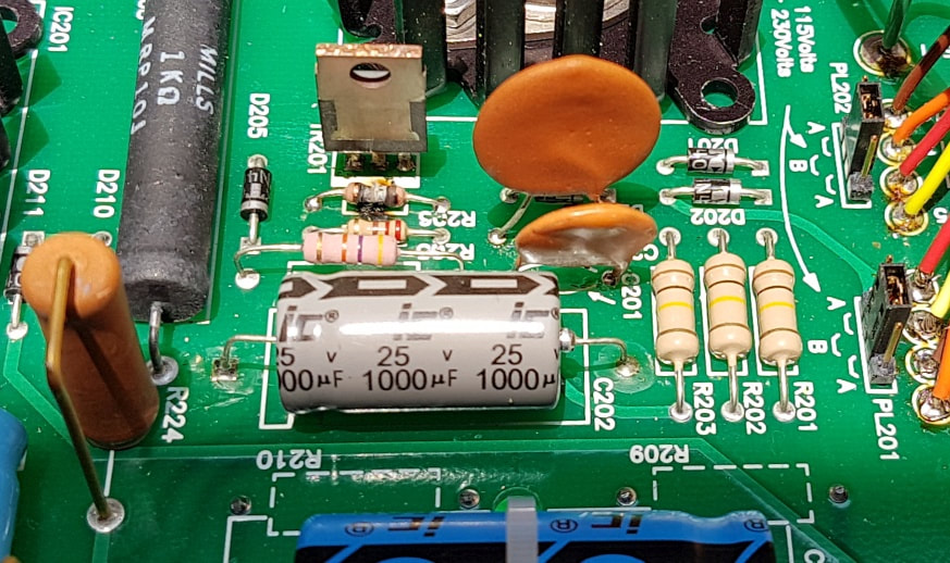
From the early inspection of the 2701C, before I carried out the modifications. The burnt resistor R206 is clear to see, but something else is wrong: The C202, here a 1000 µF / 25 V capacitor, is supposed to be a 10 µF / 350 V capacitor.
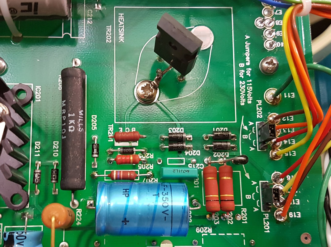
The repaired and modified power switcher for the high-voltage transformer. The transient suppressor and the snubber networks are located on the bottom of the board.
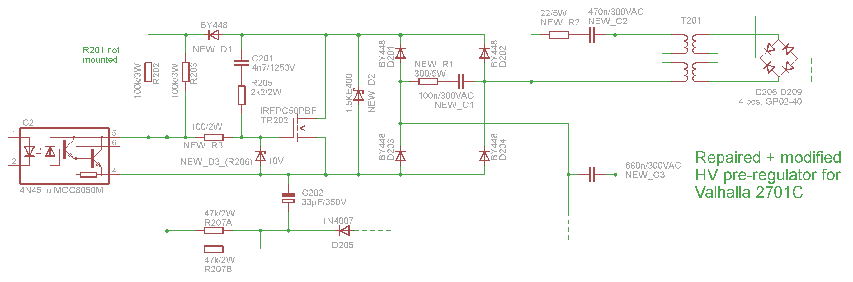
Schematics of the modified power switcher. Only attempt a similar change at your own risk!!
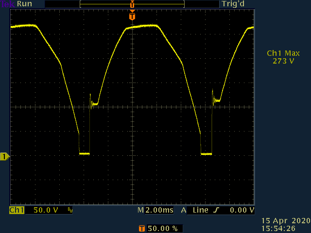
The new switcher in action for the first time, without the use of the RC feedback network to limit dV/dt, with the 2701C set to 100 V, and without load of the output. The picture shows the voltage over drain and source of the MOSFET using a Tektronix P5202 differential high-voltage probe, and with the oscilloscope grounded. The snubber network over the switcher and the transient voltage suppressor keep the level safe. Expect that the voltage of the original design will look different.
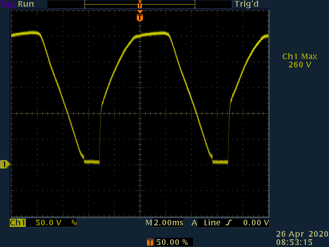
The voltage over the MOSFET, now with the dV/dt limiting RC-network (4.7 nF in series with 2.2 kOhm) in place from drain to gate of the MOSFET. Also, a snubber network (470 nF in series with 22 Ohm) over the primary of the high-voltage transformer has been added. Again, you should expect that the voltage of the original design will look different.
|
1) The switcher / pre-regulator for the high-voltage transformer
First, a word of caution: If you are going to carry out measurements of the switcher or repairing it, please beware of the high voltages inside the 2701C and of the switcher's missing isolation from the mains! Do not use ordinary oscilloscope probes for measurements of the switcher, but only probes specifically made for mains voltages in mind. For safety reasons, I also used a variac with isolation transformer to power the 2701C during the test and repair sessions. Besides the obvious missing fuse on the back panel I noticed that resistor R206 was clearly toast. Looking more closely at the 2701C it appeared that someone had tried to repair the it. As an example, the soldering job of the high-voltage bridge rectifier, made of series connected 1N4007 diodes, was not of the same standard as for other components. Furthermore, the 1N4007 diodes of the high-voltage rectifier were of a different brand than the other 1N4007 diodes in the 2701C. Finally, and to my surprise, capacitor C202, which is supposed to be a 10 µF / 350 V capacitor, was actually a 1000 µF / 25 V capacitor! Another surprise was that this capacitor had not been destroyed, perhaps due to the current-limiting resistor R208. With a burnt R206, the transistors TR201 (2N6499) and TR202 (2N6543) were to no surprise shorted. It is not clear what had caused this, but it may have been a short on the secondary of the high-voltage transformer, perhaps caused by a previous rectifier failure. All this remains guesswork, however, and to ensure proper operation of the switcher I decided not only to replace a number of components, but to do a rework of the switching circuitry. The rework was also driven by my lack of trust in the current design: For instance, the TR201 is rated at merely 350 V, which is close to the peak voltage of the mains here in Europe. Also, the design with resistors R201, R202 and R203 connected directly to the collectors prevents the transistors from turning complete on. Thirdly, it attracted by attention that there's a factory selected capactor C215 in the RC network from collector to base of transistor TR202. The RC network works as a means to limit the dV/dt as it will act as a local feedback around TR202. I decided not to look for exact replacements for TR201 and TR202, and then waste further time to check out the effect of the RC-network. Finally, R205 in the RC-network is at risk of being exposed to voltage transients approaching the peak rectified voltage. It is listed as a 0.25 W carbon film resistor, and I would not trust the voltage rating or surge capabilities of this resistor. If the switcher circuitry had worked, I would replace R205 with a resistor that would withstand that the RC network is exposed to a 350 V step. Having removed the components of the switching circuitry, I could in fact power up the 2701C ... and it worked. A separate 250 V power supply connected to the high-voltage side allowed me to run the 2701C in all ranges but the 1200 V range. I then continued building a new switching circuitry, depicted in the schematics shown to the left. In summary, these were the changes I made to the power switcher in the 2701C: New fuseholder; The fuse carrier of the old fuseholder was no longer around. C202 replaced with 33µF / 350 V (no reason for 33 µF rather than 10 µF, but I had a stock of 33 µF / 350 V capacitors). Rectifier D201-D204 replaced with BY448, which is rated at 1.5 kV High-voltage recifier diodes D206-D209 replaced with GP02-40, which is rated at 4 kV and 250 mA average. Once, the rectifier diodes in the 2701C were MR250-2, rated at 2 kV and 250 mA average, but Valhalla replaced each of these with two 1N4007 in series. However, I do not like having diodes in series without any means of distributing the voltage across them, unless the diodes are specifically documented as controlled avalanche types that allow series configuration. TR201 and TR202 were replaced with one MOSFET, an IRFPC50, rated at 600 V, and a 10 V zener diode was added in place of R206 to limit the gate to source voltage. The three resistors R201-R203, apparently 1 W film (the kind of film is not specified), were replaced with two Vishay PR03 100 kOhm / 3 W resistors with a 750 V rating. The resistor R201 was left out. A unidirectional transient suppressor 1.5KE400 was placed over drain to source of the IRFPC50. A snubber network (300 Ohm / 5 W resistor and 100 nF safety film capacitor in series) was placed across the AC side of the rectifiers. A diode BY448 was inserted before R202-R203 to prevent the gate voltage going down when the MOSFET pulls down. As a result, the MOSFET can be fully driven as intended. A replacement of the optocoupler IC2, as the output side is connected to the roasted parts of the switcher circuitry. Note that the insulation specifications of any replacement has to at least match those of the 4N45 used. In this case, I used an MOC8050M. I carried out the first checks of the new switcher without the RC-network R205, C201 and C215, but added later a series combination of 2.2 kOhm and 4.7 nF to further limit the dV/dt of the turn-off transient. The transient suppressor 1.5KE400 prevents overvoltage, so the RC network is now just an additional means of controlling the transients, and does not require a factory selection of components. Note that the RC network should not limit the dV/dt too much, as this will cause excessive loss in the MOSFET. If the edges become too slow, the MOSFET will spend too much time as a linear amplifier rather than a switch. Right now, the MOSFET runs cool and has no need for a heatsink. |
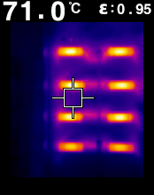
Above: The resistors R209 through R216 create hotspots when the 2701C is set to a high voltage. This effect may be somewhat suppressed by using resistors with a higher dissipation rating, though the dissipation inside the box will remain the same.
|
2) Dissipation issues
If the chain of transistors TR6 through TR12, and the resistors R8 through R12, for one reason or another, is exposed to the maximum voltage, the original resistors will endure about a 300 % power overload. The choice of power rating of the original resistors seems to be driven merely by the normal condition of about 200 V across the chain. I replaced resistors R8 through R12 (100 kOhm 0.25 W carbon film) with 100 kOhm Vishay PR02, rated at 2 W and 500 V. Another case of too low a power rating: At high voltage settings, the dissipation of the 27 kOhm bleeder/distribution resistors R209 through R216 becomes higher than the 1 W rating of the present model. With the top and bottom plates removed, the 2701C even emits a smell due to the heat. All resistors were replaced with 27 kOhm model ROX5S from TE Connectivity, rated at 5 W. As a side note, one could suspect that the dissipation in the resistors R8 through R12 could have an impact on the voltage stability at high output voltages due to the temperature rise inside the box. Hence, it should be stressed that the replacement of resistors does not lower the dissipation inside the box, but it only mitigates the hotspots identified. A lower dissipation would likely call for the use of high-voltage DC film capacitors rather than the series coupled electrolytic capacitors. Ideally, the heat-generating supplies should be thermally separated from the rest of the electronics, but that's another story... |
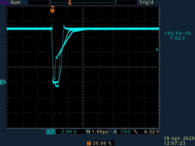
The picture above shows how the output of IC11 is shorted during the transitions of the gate control signals. To make things worse, the shorts of the IC11 introduce spikes on the +15 V and -15 V supply rails.
|
3) PWM chopper modification
During the repair of the 2701C my attention was drawn to the PWM chopper configuration with two pairs of N-channel MOSFETS driven by the complementary outputs of a 4013 D-type flip-flop. One needs to make sure that the FETs of each pair do not conduct at the same time during the transition. However, the outputs of the reference and of the buffer IC11 are in fact briefly shorted. Assuming the reference is a custom LM299, it's basically a zener sourced by a resistor, and the short should not pose a reliability issue. However, shorting the output of an operational amplifier is not a good idea. Though the amplifier may be designed to cope with shorts, there is very likely still going to be an issue with the transient current draw from the power rails. One remedy is to replace R34 with three resistors in a T-configuration, having two resistors is series between the source of the upper MOSFET and the drain of the lower. The node connecting these two resistors is then connected to a new R34. When both FETs conduct, the series connection of two resistors will limit the current draw. I replaced R34 (60.4 kOhm, 1 %, 50 ppm/K) with a 59.0 kOhm 0.1 %, 15 ppm/K resistor, connected to the center of two 1.40 kOhm, 0.1%, 15 ppm/K resistors. The change reduced the spikes on the +15 V and -15 V rails. To further improve the +15 V and -15 V rails, the decoupling capacitors C301 and C302 were inserted. They seem to be mounted only if the current output option is installed, but the limited decoupling on the 2701C could do with some help. Another issue with the design of the switcher is that the time before the voltage settles seems rather long. The settling time, which is close to 1.5 µs, is about 130 ppm of the PWM period. Any difference in the rising and falling edges will result in an offset, and if the edges change with the setting it will upset the linearity. The design goal would be to have equal rising and falling edges that do not change. With a setting time of about 1.5 µs a change of just 1% of either the falling or rising edge will result in a change in the order of 1 ppm. However, an improvement of this would likely involve too many changes of the switching circuitry that I care to make, so I decided to leave the MOSFET configuration as it is. |
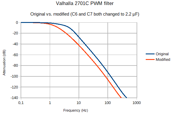
Simulation of the filter characteristics: The original filter, and the filter with the increased capacitor values. The theoretical improvement at the chopper frequency is 13.7 dB.
(Picture to be added)
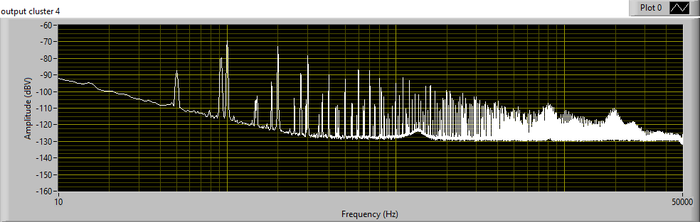
Output spectrum, at 100 V out in the 120 V range, before and after the modifications. |
4) PWM clock feedthrough
A measurement of the output spectrum revealed some feedthrough from the PWM chopper frequency, and its harmonics, especially at high output voltages where the amplification is high. The first item that crossed my mind was the PWM lowpass filter. An analysis in LTspice showed that the attenuation could be improved without increasing the settling time significantly. By about doubling the values of C6 and C7 we get about 4 times better attenuation at the chopper frequency, at least in theory, and a nice roll-off. I changed both C6 and C7 from 1 µF / 50 V to 2.2 µF / 160 V, and I checked both of the new capacitors for leakage. The insulation resistance was above 20 GOhm, slighty better than the old capacitors. To my disappointment, the filter modification reduced the RMS noise by only 2.5 dB, measured at 100 V, with the harmonics of the clock still being clearly present in the spectrum, so the PWM clock must couple to the output through some parallel path. I realized that some unwanted coupling could be caused by the resistor pair R38A and R38A: One end of R38A is connected to the node which has full PWM amplitude, and one end of R38B is connected to the feedback node of the chopper amplifier IC5. The resistor pair is placed next to each other, which inevitably will result in some capacitive coupling. In order to mitigate this I placed a grounded screen between the two resistors. This did in fact lower the level at the PWM clock frequency, but only with about 3 dB. On the other hand, it proves that the coupling between R38A and R38B indeed is an issue. In view of the limited improvements, I suspect that a major contributor to the PWM clock feedthrough is the actual layout of the 2701C: The analog ground is distributed unevenly, and this makes it difficult to ensure that the different nodes in the circuit reference properly to the analog ground. Another example is that the chopper amplifier IC5 is located far away from the PWM filter, which makes the net of the feedback node rather large, and again, it makes proper referencing to the analog ground difficult. In all, I decided not to pursue further reductions of the PWM clock feedthrough. |
The results
Summary to be made ....
Summary to be made ....
|
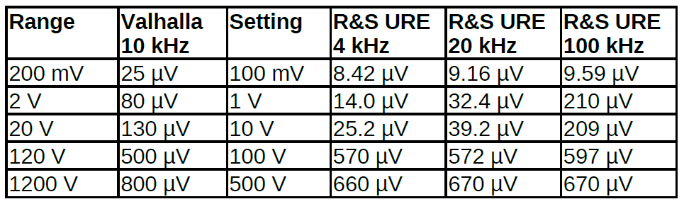
Above: The RMS "wideband" noise as specified by Valhalla (in a 10 Hz to 10 kHz range) is listed in the second column. The measured noise as measured by a Rohde & Schwarz URE RMS voltmeter with an EG&G amplifier with 100x gain in front for the all but the highest range, and for different bandwidth settings, is found in the last three columns. The 120 V range seems to have an issue with too high a noise level, though one should note that the original design may perform differently. Still, it's fair to say that the 2701C does not have a very low noise level.
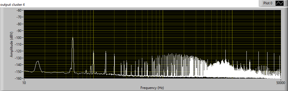
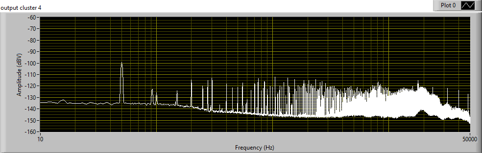
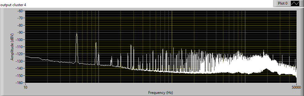
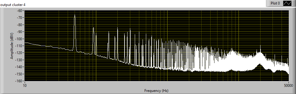
To the left: Noise spectrums of the 2701C, after having gone through the repair and modification session, from top to bottom:
100 mV in the 200 mV range 1 V in the 2 V range 10 V in the 20 V range 100 V in the 120 V range 500 V in the 1200 V range In the 4 lower ranges an EG&G model 113 amplifier set to 100x gain was inserted between the output of the Valhalla 2701C and the input of the NI USB-4431 digitizer. There's a wealth of spectral components originating from the mains and from the PWM frequency, and I suspect a redesign of the layout is required to lower this. Also, there seems to be an increasing amount of 1/f or flicker noise at the higher voltage ranges, which I believe originates from the LMx99-type reference. These ranges could benefit from an optional low-pass filter with a cut-off somewhere between 0.1 and 1 Hz. |
|
GPIB option for 2701C
It does not require many knob-twisting exercizes before one desperately would like to be able to adjust the voltage through GPIB. Unfortunately, my unit did not come with the TL-3 option, which includes GPIB and an additional interface to control the Valhalla 2500EP current calibrator. However, as the schematics of the TL-3 option is available on the Internet, I decided to run my own spin. The design is by large a copy of the original TL-3 with these differences: I use the SN75ALS160DW and the SN75ALS162DW as interfaces, both in SO-package as 'DW' suggests, I have added transient suppressor CDNBS16-T05 (unidirectional 8-channel in SO-package), and the GPIB connector CIB24SPC from L-Com (available from eg. Pidso in Austria). The PNP outputs for the 2500EP have been protected with transient suppression, using either unidirectional transient suppressors or common zeners. Also, there's a few other choices of the passives. The grounding strategy differs from the original TL-3, as the connector shells are connected to the chassis, while the digital ground is only connected galvanically to the board through the flat cable. In an attempt to suppress potential RF interference the GPIB module's ground is decoupled to the chassis through capacitors, and a ferrite for the flat cable has been added close to the GPIB module. |
|
Linearity test
With a PWM-based design, one should expect a high degree of linearity, though with some effects arising from the fact that there are two PWM-strings, and likely from the range of implementation details, especially related to the chopper. The graph to the right shows the results of the first linearity test, carried out around 10 V in the 20 V range, in steps of 10 µV. The voltage from the 2701C was compared to a Fluke 731B, and the difference was measured by a Fluke 8842A in its 20 mV range, as an average of the 5 central values out of 7 measurements. When taking the measurements, my 2701C did not have GPIB option, so each of the 401 voltages of the measurement session had to be set by hand. Note what appears to be an outlier around 9.9983 V. After the home-made GPIB option was installed, the test was repeated, but this time by measuring the voltage directly with a HP 3458A multimeter. A voltage sweep was repeated 18 times, and the 16 center values for each set point were averaged. There was a waiting period of 500 ms after each setting, and 5 s after the first setting in a new sweep to allow proper settling of the 2701C. Furthermore, there's a waiting period of 5 min before the very first measurement is taken, as the 2701C needs time to settle once the output is activated, even when it has been powered up hours before. As you may see, there's a resemblance between the first linearity measurement and the more elaborate second one, but the features of the error graph are now clearer to see. As one could expect, the error has shifted due to the difference in calibration of the 731B and the 3458A, to different offset voltages in the two setups, and due to drift over time of the 2701C. Interestingly, what was initially assumed to be a measurement outlier around 9.9983 V is seen again, and we may now actually assume that this is a feature of the 2701V. The repeated "humps" of the graph can be explained by the misalignment of the two PWM strings of the 2701C. I have not (yet) found an explanation for the remaining features of the voltage error graph. |
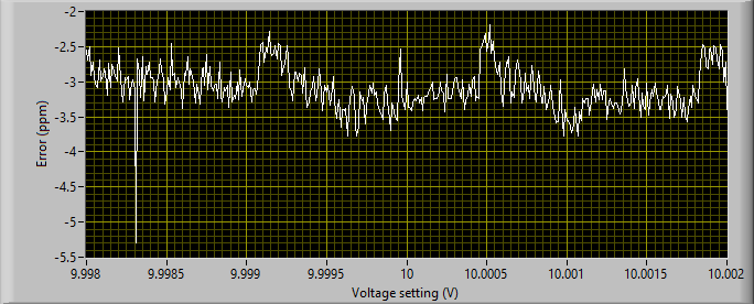
The first test of 2701C linearity: A manual selection of voltages from 9.998 V to 10.002 V, and the voltage compared to a 10 V reference, the Fluke 731B, using a Fluke 8842A multimeter.
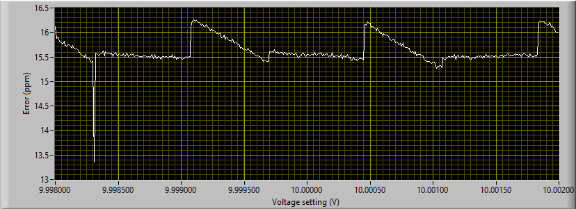
Results from the improved linearity setup: The average of 16 rounds, measured with the HP 3458A, using automated setup of the 2701C through GPIB. The control and the data handling were done in LabVIEW.
With a resolution of 1 ppm (at 10 V) and an observed error jump of close to 2 ppm, one has to conclude that the 2701C is not monotonous for all settings. |
|
The interesting findings of the linearity test above encouraged me to test other ranges. The graph to the right shows the results of a voltage scan from 4.4 to 4.5 V in steps of 100 µV, a total of 1000 individual voltage settings. Again, the voltage was made with a 3458A multimeter, and over 18 voltage scans, using the average of the 16 middle values for each setting.
|
|
(Picture to be added)
|
Drift vs. Fluke 531B, both set to 10 V, with measurements captured by a Keithley 181 nanovoltmeter once per second. The 181 was in its 2 mV range, with its filter and damping enabled. The Fluke 531B had been powered on for more than a year, and the Valhalla 2701C had been powered up 24 hours before the measurement session started.
|
Final remarks
So, based on the above, if you have a 2701C in its original condition and still working, I would recommend that you consider the following basic changes, only as an effort to increase the reliability:
Replace resistors R8 through R12 with model rated at 1 W or more, and with a specified max. voltage of at least 500 V.
Replace the series coupled 1N4007 rectifier diodes in the high-voltage supply with proper high-voltage diodes, rated at least at 3 kV and 250 mA average, or use series coupling of diodes that have documented controlled avalanche properties.
Replace the 27 kOhm bleeder/distribution resistors R209 through R216 with a model of a higher power rating, preferably 3 W or more.
Replace R34 with a T-configuration to prevent brief shorts of the IC11 output, as described above.
Add capacitors C301 and 302 for decoupling.
Finally, check that C202 has the value it is supposed to have!
At least in 230/240 V countries, consider also these changes:
Replace resistors R201 through R203 with a model rated at 2 W or more, and with a specified max. voltage of at least 500 V.
Replace R205 with a surge capable resistor, and with a specified max. voltage of at least 500 V. An example could be the TE Connectivity EP series.
The voltage rating of transistor TR201 is marginal, and ought to have a higher rating when the 2701C is used in 230/240 V countries. However, replacing it may have a negative impact on the function of the dV/dt limiting RC-network. I would only consider replacing it if your mains voltage is at the high end, and if you have the means to verify the function of the switcher and the effect of the RC-network.
